


Sensor Packaging: Critical MEMS Considerations
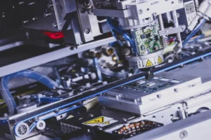
Die bonding of MEMS devices for package assembly.
Sensor packaging, particularly for microelectromechanical systems (MEMS), is a critical aspect of modern electronics. MEMS developers have demonstrated a variety of innovative microsensors for almost every possible sensing modality including temperature, pressure, inertial forces, chemical species, magnetic fields, radiation, etc. While MEMS sensors are revolutionizing various industries with their precision and miniaturization, they can present unique product development challenges and risks during design, development, and manufacturing.
There are several critical decisions to be made that accommodate the intricacies of MEMS packaging and ensure performance of these sensor-driven devices.
Material Selection Considerations
- MEMS sensors are highly sensitive to mechanical stresses. Careful attention must be paid to temperature ranges required to package the MEMS device as many materials used in packaging have large coefficient of thermal expansion (CTE) mismatches with the materials constituting the MEMS sensor. Stresses resulting from CTE mismatches can be very large and scale with the magnitude of temperature changes during processing. Problems arise when these factors aren’t considered — issues that can significantly impact sensor yield, performance, and reliability. Therefore, it is critical to select appropriate materials and processing temperatures to minimize mechanical stresses induced by CTE mismatches. Best practices suggest employing packaging materials with low thermal expansion coefficients to prevent mechanical stresses that could lead to sensor failure. It’s important to select materials carefully to ensure that components react appropriately under stresses as they heat up and cool down during packaging processing. The more that CTEs match between adjoined materials, the more similarly the components will expand and contract when exposed to varying thermal conditions, either through processing or environmental factors.
- Other selection considerations include choosing materials that provide protection for the sensor while also ensuring its optimal performance. Environmental conditions in which the sensor will ship, store, and operate must be considered. Factors such as humidity, temperature extremes, rate of ambient temperature change, and exposure to chemicals should influence material choice. For example, hermetic sealing can be employed to protect sensors from moisture and other environmental contaminants, ensuring long-term reliability. Hermeticity is needed for medical devices, especially implant-ables, to protect the device from the various fluids in the human body that could cause corrosion and shorting. It also protects the patient from toxic or harmful materials being released from the device.
Handling During Manufacturing
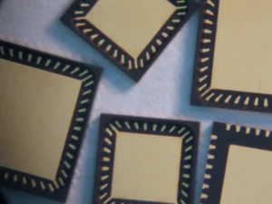
Air cavity packages are ideal for MEMS and sensor devices.
- During manufacturing, MEMS sensors require careful handling to prevent damage. The devices are often flexible but must be kept rigid during processes like ultrasonic interconnect attach via flip chip or wirebond and custom pickup tools, fixtures, and jigs. Proper handling of the MEMS is required to reduce and eliminate damage and maintain sensor integrity. Manufacturing processes should be designed with the sensor’s fragility in mind to avoid mechanical stresses that could impair its performance.
- MEMS sensors often require air cavity packages or exposed silicon on a board to function correctly. These configurations provide the necessary environmental exposure for the sensors to operate. However, protecting the wirebonding interconnect to these delicate structures is paramount. Encapsulation using techniques such as dam and fill or film-assisted overmolding can protect the wirebonds from contaminants and mechanical damage while preserving an opening for the sensor to function properly. This process involves creating a barrier around the sensor to shield it from epoxy material, used to protect the wirebond interconnects, while ensuring that the sensor’s functionality is not compromised. The encapsulation process must be meticulously designed to maintain sensor functionality while providing robust protection.
Process Development and Validation
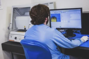
Accurately measuring materials and dimensions is essential for developing robust manufacturing methods.
- Interconnect technology can play a significant role in MEMS sensor packaging. Flip chip and wirebond are two common interconnect methods used to establish electrical connections between the sensor and the package. Each method has its advantages and considerations. Flip chip interconnects offer higher density and better electrical performance in a smaller package size, while wirebonding is a more established technology and offers more architectural flexibility, making it popular for MEMS and sensor devices. The choice of interconnect method depends on the specific requirements of the sensor application and the desired performance characteristics.
- Wafer processing poses specific challenges for MEMS sensors, particularly due to the fragile nature of MEMS sensors and process steps inherent in wafer singulation. Designing sensors with manufacturing processes in mind can mitigate these risks. This includes considering the mechanical stresses and selecting suitable singulation methods that minimize damage during wafer cutting.
- The methods and workflows of a MEMS saw singulation process should also be considered; different singulation methods should inform design and process flow, such as when to singulate devices, how to process the MEMS die, and whether saw or laser singulation is required. Saw singulation involves wafer tapes and the continuous spraying of deionized (DI) water due to high friction. Both elements of traditional saw singulation run a high risk of causing significant damage to MEMS devices because of their varying complexity and fragility. Depending on which surface of the MEMS contains the functional elements, the wafer tapes could pull way and damage key components. The DI water spray often has enough force to damage MEMS as well, depending on water pressure and blade wheel speed. A great alternative is laser dicing, which still uses wafer tapes but does not use DI water, minimizing the risk of damage to a wafer during singulation. However, this process singulation method usually requires narrower saw streets and thinner wafers.
Developing and validating manufacturing processes for MEMS sensors requires careful planning, expertise, and proper equipment sets. A dedicated process development stage is necessary to fine-tune manufacturing steps, take precise measurements, and perform destructive testing to validate the process. These ensure that the sensors meet performance and reliability standards. Using mechanical parts and coupons as substitutes for expensive, functioning parts during validation can help reduce costs and streamline the development process.
MEMS sensor packaging is a complex and multifaceted process that demands careful consideration of various factors. By addressing these challenges through innovative techniques and meticulous process development, the potential of MEMS sensors can be fully realized. Ensuring robust protection and optimal performance of these sensors paves the way for their continued integration into diverse applications, driving technological advancement and enhancing the capabilities of modern devices.
Article source: Medical Design Briefs